Guaranteed Higher Grade!
Free Quote
Task:
Part 1: Design a combinational complete adder circuit system using CMOS integrated circuits inside a digital arithmetic framework.
Examine the circuit's functionality at each logic level. Utilize data sheets to compare the parameters of your circuit using AND, OR, and Exclusive OR gates. Authenticate your evaluation using truth tables.
Assess the distinctions in the operation of sequential and combinational logic devices inside a Full Adder Circuit.
Part 2: Evaluate and propose modifications to the circuit process of a digital system concerning the data collection methodology and the used interface. Considering the alarm system used for the measurement, monitoring, and performance optimization of the circuit.
Comprehend and evaluate the operational mechanisms of the system regarding information collection and dissemination of discoveries within its service, highlighting potential enhancements.
Comprehend and suggest improvements to the human engagement with the Full Adder Circuit.
Response
Digital Logic Circuit: Distinct voltage levels must be used for the operation of digital logic circuits. Digital circuits use abstract circuit elements. Gates are referred to as the abstract elements of the circuit. The output of the gate is the input variable. Digital circuits mitigate noise interference and signal degradation inherent in analog circuitry. There are two categories of digital circuits:
Combinational Logic Circuits
The output of a combinational logic circuit is a function of the current inputs. Consequently, a combinational complete adder circuit cannot hold a state. Combinational logic circuits execute calculations on stored data. Various types of combinational logic circuits, including multiplexers, de-multiplexers, half adders, full adders, encoders, and decoders, are available. The Sum of Products (SOP) and Products of Sums (POS) methodologies are used to implement combinational logic circuits. Combinational logic circuits lack storing memory. Introducing a new input to the combinational logic loop will result in the deletion of the prior input data.
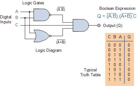
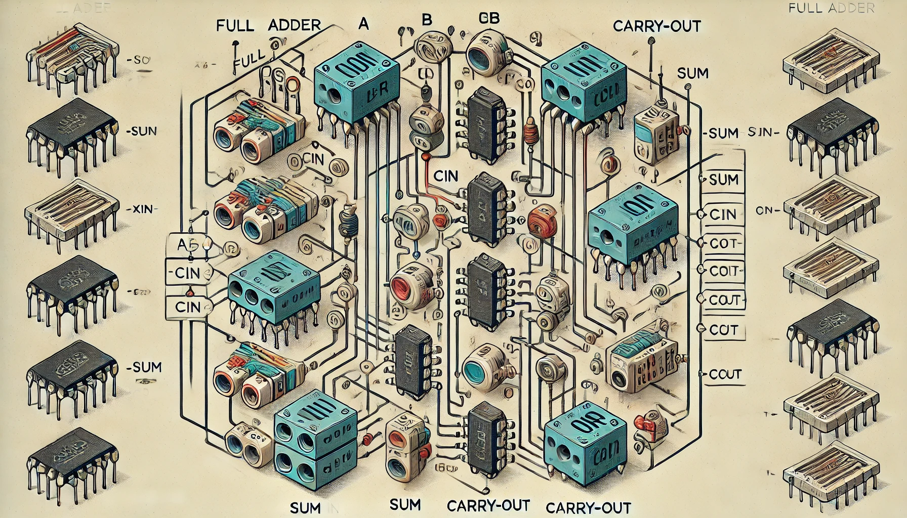
Figure 1: Complete Adder Circuit, Truth Table, and Boolean Expression
Sequential Logic Circuits
Output is contingent upon both current and previous inputs in sequential logic circuits. Information is retained in a digital circuit using sequential logic circuits, with memory housed inside these circuits. A latch is the most fundamental component of a sequential logic circuit. Latches may be referred to as flip-flops. The loop is defined as a combination circuit in which one or more outputs are fed back as inputs. Commonly used are SR (Set–Reset), JK, T (Toggle), and D flip-flops. Sequential logic circuits are used in every cycle for memory components. Clock signals are used in sequential logic systems. It initiates the flip flop process.
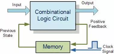
Figure 2: Block Diagram of a Combinational Logic Circuit
|
Sequential Logic Circuits |
Combinational Logic Circuit |
|
There are components of memory in it. |
There are no components of memory in it. |
|
The current output value relies on the inputs value and past value. |
The existing output value relies on the current input value. |
|
It is possible to store the information in digital circuits. |
It is not possible to store information in digital circuits. |
|
They are clock-independent. |
They rely on the clock. |
|
There is a need for feedback circuits. |
There is no need for feedback circuits. |
Alarm system used for the measurement, assessment, and detection of defects and necessary modifications.
The support structure is used to manage atypical situations. This kind of aid is designated as the alert system. It serves as the primary support foundation for the operator. The user is notified of the system's irregularity. The alarm system can anticipate the danger. The alarm system serves to alert, inform, and guide the user on an anomalous event. The suitable reaction should be specified at this time. The user must be able to resolve the challenges at a comprehensible pace. The alarm system must be operational under all circumstances. It must be meticulously crafted. The fault finder tracker is used to locate the flaw. In the event of a fault in any line, the alert can pinpoint the location of the issue. The alarm system, often identified as the smoke detector, is used to sense smoke.
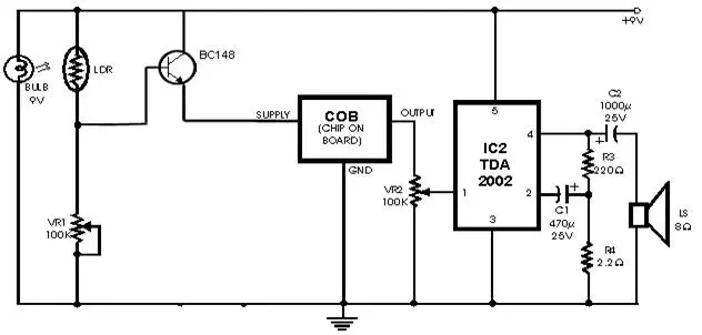
Figure 3: Smoke Detector Circuit
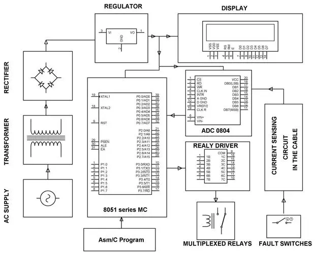
Figure 4: Circuit schematic of subterranean cable fault distance finder
If a flaw is found in an underground wire, the circuit above may detect it. Identifying the location of the defect for rectification is essential. This adheres to the notion of Ohm's law. This use the 8051 microcontroller. The ADC unit computes the wire length (in kilometers). An integrated circuit for relay driving controls the relays. The wire connections are evaluated using it. A microcontroller is connected to an LCD unit for data reading. Various electrical or physical parameters are computed using a certain methodology. This technique is referred to as Data Acquisition (DAQ). The variables computed by DAQ include sound, voltage, pressure, current, and temperature.
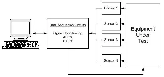
Data Acquisition Block Diagram
The preceding block diagram delineates the data collecting method for the monitored equipment. Various sensors are affixed to the device. DAQ connects these sensors to a computer. The circuit update has been commissioned by DAQ. Upon inspection of the gadget, this enhances its quality and functionality. It may also enhance the efficacy of the subterranean wire fault locator. When the microcontroller is connected to the DAQ circuit and alarm system, the alarm system may promptly detect the error and simultaneously display the location of the defect on the screen. It will enhance the system's performance and dependability.
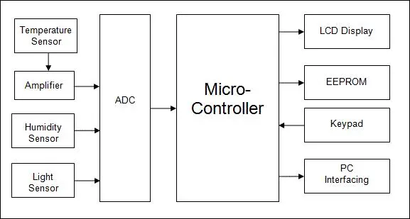
Figure 6: Data Acquisition System with the 8051 microcontroller
The preceding page displayed the schematic of a data acquisition system using the 8051 microprocessor. The figure illustrates all the needed tools. To enhance its efficiency, a system must possess all necessary equipment. Connecting the microcontroller to the DAQ circuit will facilitate the device's information retrieval. The human interface in any software is crucial. Humans should interact well with computers to enhance the device's effectiveness. The user interface is the only means to connect the other devices. Consequently, all requisite devices inside a network must be interconnected to enhance application efficiency. Our electrical engineering assignment assistance specialists from prestigious colleges are preparing full adder circuit assignments, enabling us to provide a dependable top-tier assignment aid solution.
Bibliography
VanCamp, K. (2016). Alarm management by the numbers. Chem. Eng. Essentials CPI Prof., Autom. Control.
Larsson, J. E., Öhman, B., Calzada, A., Nihlwing, C., Jokstad, H., Kristianssen, L. I., ... & Lind, M. (2006, November). A revival of the alarm system: Making the alarm list useful during incidents. In Proceedings of the 5th International Topical Meeting on Nuclear Plant Instrumentation, Controls, and Human Interface Technology, Albuquerque, New Mexico.
Bransby, M. L. (2000). Best practice of Full Adder Circuit in alarm management.
Leva, M. C., Naghdali, F., & Alunni, C. C. (2015). Human factors engineering in system design: a roadmap for improvement. Procedia CIRP, 38, 94-99.
John, M., Joseph, A., & Vasanthi, D. (2017). Design and implementation of low cost Full Adder Circuit in multichannel data acquisition hardware for computer aided measurement. In 2017 Trends in Industrial Measurement and Automation (TIMA) (pp. 1-4). IEEE.
Hypolite, K., Wolf, J., Brun-Kestler, A., & Brun-Kestler, M. (2015). U.S. Patent Application No. 14/583,710.
Piccolo III, J. (2015). U.S. Patent No. 8,988,217. Washington, DC: U.S. Patent and Trademark Office.

Get original papers written according to your instructions and save time for what matters most.
Order Now